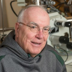
Roy Geiss, an electron microscope expert in the university’s Central Instrument Facility, has been honored by the National Institute of Standards and Technology for his invention of a groundbreaking technique in analytical microscopy.
Geiss received the Materials Measurement Laboratory Distinguished Associate Accolade for his invention of transmission electron backscattered diffraction, or t-EBSD. Geiss was honored at a June 6 gala in Boulder.
The technique for which he was honored provides a tenfold improvement in the spatial resolution of mapping orientation and structure of crystalline materials, compared with the conventional technique. With this development, Geiss has provided the research community with a powerful tool for characterizing materials used in advanced electronics, nanotechnology and nano-crystalline structural alloys.
Geiss’ research interests include a wide variety of hard and soft materials. He uses transmission electron microscopy and scanning electron microscopy, as well as associated techniques including electron diffraction and energy-dispersive X-ray spectroscopy.
Geiss was previously employed at the National Institute of Standards and Technology as a materials research engineer. He has a doctorate in applied physics from Cornell University, and also served as a research scientist at IBM’s research division before joining CSU’s Central Instrument Facility. The facility is housed in the Department of Chemistry and is a foundational core research facility supported by the Office of the Vice President for Research.